

MOSFETs are the backbone of countless modern electronic systems, and engineers who work with them know that even small oversights can lead to frustrating failures, wasted components, and costly redesigns. Among the many transistors available today, the 2N5458 stands out as a reliable N-channel MOSFET widely used in switching, amplification, and signal processing applications. Yet despite its popularity, engineers frequently encounter problems that stem not from the component itself, but from avoidable mistakes in selection, circuit design, and thermal management.
Whether you are an experienced designer or just becoming familiar with N-channel MOSFET behavior, understanding where things typically go wrong is the first step toward building circuits that perform consistently and last. This article walks through the most common errors engineers make when working with the 2N5458, from misreading datasheets and poor biasing decisions to inadequate heat dissipation and flawed testing methods. For each pitfall, you will find clear, actionable guidance to help you correct course and get reliable results from this capable component.
Understanding the 2N5458 MOSFET: Key Specifications and Characteristics
The 2N5458 is a junction field-effect transistor (JFET) — specifically an N-channel device — that has earned a steady place in analog circuit design due to its low noise characteristics and predictable behavior across a wide range of operating conditions. Engineers commonly deploy it in audio amplifiers, voltage-controlled attenuators, analog switches, and high-impedance buffer stages where signal integrity is paramount.
Getting the most from this component starts with a firm grasp of its core specifications. The 2N5458 operates with a drain-to-source voltage rating of 25V and a gate-to-source voltage range of ±25V, setting hard boundaries that circuit designers must respect to prevent breakdown. Its continuous drain current is rated at 9mA, which makes it well suited for small-signal work rather than high-current power applications. The gate threshold — more precisely, the pinch-off voltage (Vp) — typically falls between -0.5V and -6V, a notably wide range that demands attention during biasing since individual units can vary significantly within that window. Forward transconductance (gfs) ranges from 2.0 to 9.0 mS, directly influencing gain calculations in amplifier stages.
Power dissipation is rated at 310mW at 25°C ambient, a figure that drops with rising temperature according to the device’s derating curve. Ignoring this relationship is a frequent source of premature failure. Understanding that the 2N5458 is a JFET — not an enhancement-mode MOSFET — also matters, since it conducts at zero gate bias and requires a negative gate voltage to reduce drain current, behavior that surprises engineers accustomed to working with standard N-channel enhancement transistors.
Common Mistakes in Selecting and Sourcing the 2N5458
Selecting the right component begins long before a circuit is assembled, and the 2N5458 is no exception. One of the most persistent errors engineers make is misreading the datasheet — specifically, treating the pinch-off voltage as a fixed value rather than a range. Because Vp can span from -0.5V to -6V across different units, a design that works perfectly with one batch may behave erratically with another. Always design your biasing circuit to accommodate the full specified range, not just the typical value shown in application examples.

Environmental factors are another overlooked consideration during component selection. Engineers often specify the 2N5458 for an application without accounting for the operating temperature range of the final product. The device’s 310mW power rating applies only at 25°C, and performance characteristics like transconductance shift meaningfully at elevated temperatures. Before finalizing your selection, verify that the component’s rated conditions align with your actual deployment environment, particularly in automotive, industrial, or outdoor applications where temperatures fluctuate widely.
Sourcing from unreliable vendors introduces a separate but equally serious risk. Counterfeit and substandard JFETs are common in the secondary market, and they often pass basic visual inspection while failing under real operating conditions. To protect your design, source the 2N5458 exclusively from authorized distributors or manufacturers with verifiable supply chains — platforms like UTSOURCE, which specialize in electronic components with traceable sourcing, can be a practical starting point for verifying supplier legitimacy. When evaluating a new supplier, request batch test data and cross-reference the published specifications against your application requirements using a curve tracer or parameter analyzer before committing to a large order. Checking for proper date codes and manufacturer markings on the package is a quick first screen that filters out obvious counterfeits before they reach your bench.
Circuit Design Errors with the 2N5458 and How to Avoid Them
Biasing and Gate Drive Configuration Mistakes
Because the 2N5458 is a depletion-mode JFET, it conducts at zero gate bias, which catches engineers off guard when they apply biasing strategies borrowed from enhancement-mode MOSFETs. The most reliable approach is self-biasing: place a source resistor sized to develop enough voltage to bring the gate-source junction into the desired operating region, accounting for the full Vp range. Always include a gate resistor — typically between 1kΩ and 10kΩ — to limit current during transients and provide a discharge path that protects against electrostatic damage. The 2N5458’s gate is sensitive to ESD, so handle it with grounded wrist straps, store it in conductive foam, and add a small gate-to-source resistor in the final circuit to bleed off accumulated charge before it causes irreversible oxide damage.
Load Handling and Switching Performance Issues
Inductive loads present a particular hazard with the 2N5458. When the device switches off, the collapsing magnetic field in an inductor generates a voltage spike that can easily exceed the 25V drain-to-source rating, destroying the transistor instantly. Placing a flyback diode across any inductive load eliminates this risk. For resistive switching applications, excessively slow transition times force the device to linger in its linear region, where power dissipation peaks — a snubber circuit or a gate drive with a lower source impedance can sharpen transitions and reduce thermal stress. Always verify that your expected load current remains within the 9mA continuous drain current rating; exceeding this limit, even briefly under transient conditions, pushes the device outside its safe operating area and accelerates degradation.
Power Management and Thermal Dissipation Pitfalls
Thermal management is where many otherwise well-designed 2N5458 circuits quietly fail. The device’s 310mW power dissipation rating applies strictly at 25°C ambient — a condition that rarely reflects real-world operating environments. As temperature rises, the maximum allowable dissipation decreases according to the device’s derating curve, which specifies a linear reduction above 25°C. Engineers who ignore this relationship and design right up to the 310mW ceiling leave no thermal margin, setting the stage for gradual degradation or sudden failure when ambient temperature climbs even modestly.
Calculating actual power dissipation in your circuit is straightforward but frequently skipped. Multiply the drain-to-source voltage by the drain current at your operating point to get the dissipated power, then add any gate-related losses. Once you have that figure, compare it against the derating curve for your expected maximum ambient temperature — not room temperature. If the result leaves less than a 20% margin, revisit your operating point or improve your thermal management strategy before the board ever reaches production.
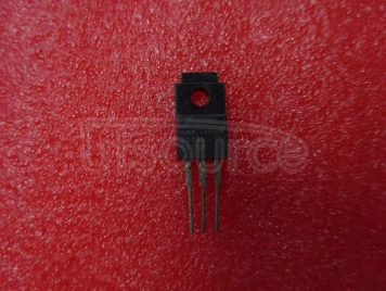
Because the transistor 2N5458 is packaged in a small TO-92 case, its thermal resistance from junction to ambient is relatively high, typically around 357°C/W. This means even modest power levels can push junction temperature toward its 135°C maximum if airflow is limited. For applications where the device dissipates more than 150mW continuously, consider mounting it with a small clip-on heatsink designed for TO-92 packages, improving airflow across the component, or repositioning it away from other heat-generating components on the board. Monitoring junction temperature during thermal qualification testing — using an infrared thermometer or a thermocouple attached near the package — gives you direct confirmation that your design stays within safe limits across the full operating temperature range.
Testing and Troubleshooting the 2N5458: Best Practices
Even a well-designed circuit can behave unexpectedly, and knowing how to test the 2N5458 correctly separates a quick diagnosis from hours of frustration. One of the most common mistakes engineers make is reaching for a standard multimeter and applying the diode-test mode as if the device were a bipolar transistor. Because the 2N5458 is a JFET, this approach yields misleading readings. Instead, use your multimeter to verify the gate-to-channel junction behaves like a diode in one direction while showing high impedance in the other — any low-resistance reading in both directions signals a damaged gate or a shorted device.
For dynamic performance analysis, a multimeter alone is insufficient. Connect an oscilloscope to the drain node while driving the gate with a known signal source, then observe switching transitions directly. Slow rise and fall times, unexpected ringing, or asymmetric waveforms each point to specific problems: excessive gate resistance, parasitic inductance in your layout, or a device operating outside its linear region. Compare captured waveforms against your simulation predictions to isolate whether the fault lies in the component or the surrounding circuit.
When troubleshooting failure modes, check first for gate oxide damage — a gate that no longer controls drain current indicates ESD-induced breakdown, which is irreversible. A drain-to-source short with no gate control points to thermal overstress. To systematically confirm device health, measure IDSS at zero gate bias and compare it against the datasheet range of 2mA to 9mA. A reading well outside this window confirms the unit is defective and should be replaced before further circuit-level diagnosis continues.
Design Discipline for Reliable 2N5458 Performance
Working reliably with the 2N5458 comes down to disciplined attention at every stage of the design process. The mistakes covered here — misreading the pinch-off voltage range during selection, sourcing from unverified suppliers, applying incorrect biasing strategies, underestimating thermal derating, and reaching for the wrong test equipment — are all avoidable with the right knowledge and habits in place. None of these errors are exotic; they appear repeatedly across projects precisely because they seem minor until a circuit fails in the field.
The most effective protection against these pitfalls is treating the datasheet as a design constraint document rather than a reference card. Design your biasing for the full Vp range, calculate dissipation against your actual maximum ambient temperature, protect the gate from ESD at every handling step, and verify device behavior with appropriate instrumentation before committing to production. These practices apply equally well to similar JFETs and small-signal transistors you may encounter in your work.
Applying these solutions consistently will not only improve the reliability of circuits built around the 2N5458, but will sharpen the broader design discipline that prevents costly redesigns and component failures across all your projects. The goal is always a circuit that performs predictably from the first prototype through the full production run.