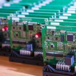
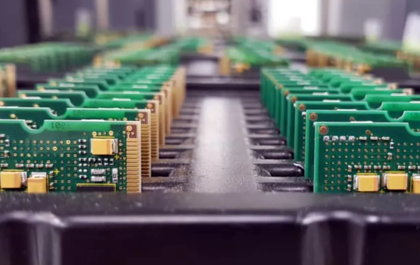
When thinking about electronic applications, there is one element that is usually integral: the printed circuit board. A PCB is necessary for bringing life to electronic devices, and this is done by routing circuit signals and ensuring they function correctly. Yet, how are PCBs designed and manufactured successfully? The following post will detail the five key steps it involves.
1. Etching the PCB
When creating a PCB, a copper layer is bonded over the substrate. An etching process, which uses a temporary mask to protect areas, is performed to remove the PCB’s excess copper. The process of etching begins by using specialist software to come up with a suitable design. Then it involves sanding the copper plate, cleaning it with a combination of water and rubbing alcohol, and cutting out the design accurately. You also have to use suitable tools to drill the necessary holes into the PCB.
Once the etching is done, the board is left with the copper traces that are desired for the functionality of the circuit.
2. The strip process
Unwanted copper will still remain on the PCB following the etching process. Either lead, tin, or electroplated tin will then cover this copper. To remove this effectively – and ensure the copper circuit underneath maintains its integrity – nitric acid is used. The use of nitric acid ensures a distinct and clear copper outline is achieved. A manufacturer can then move on to the next step.
3. Solder resist
It can be underestimated, but the use of solder resist is one of the most essential steps during the manufacturing of PCB boards. This solder resist material is used to cover up any areas which are unsoldered. The result: it stops any traces being formed by the solder, which ensures there are no shortcuts neighboring the component leads.
4. Built to be waterproof
Water can be disastrous to the function of a PCB. While the exterior of the intended device will aim to prevent water from entering, it’s not always possible. This is why it’s necessary to produce PCBs with waterproof material.
Due to the delicate nature of PCBs, this has to be done with the right care and attention. Most will turn to polymer coatings as a waterproof solution, looking to specialist polymer manufacturers for the materials to create these coatings. As well as being effective in stopping water from impacting the PCB, it is transparent, lightweight, and doesn’t corrode the copper.
5. PCB testing
Once the PCB is manufactured and seemingly ready to use, it’s important to perform testing. This testing allows you to see if the PCB functions as expected and all features work. If it’s not, the manufacturer will have to go back to the drawing board before assembling the PCB within its intended device.
Several advanced testing equipment solutions are used for this process. When it comes to high-volume PCBs, for example, these will be checked with an ATG test machine that uses fixtureless testers and flying probes.