
Modern receivers are expected to cover wider frequency ranges, capture more instantaneous bandwidth, process multiple carriers, and adapt to changing standards without rebuilding the entire analog signal chain. Faster converters and more capable FPGAs now allow you to move digitization closer to the antenna, but that freedom does not make the architecture decision automatic.
You can place the conversion point after an analog IF stage, at I/Q baseband, or directly behind the RF front end. Each position shifts complexity into a different part of your system. A superheterodyne chain preserves strong analog selectivity but adds mixers, local oscillators, and IF filtering. A zero-IF design reduces those stages but introduces DC offset, LO leakage, and I/Q balance challenges.
Direct RF sampling offers wider digital flexibility, software-defined channel selection, and easier multi-carrier processing, while demanding more from ADC input bandwidth, clock jitter, dynamic range, data interfaces, FPGA resources, and thermal design. The real question is not which architecture looks newest, but where you can control complexity most effectively. When should your receiver remain superheterodyne or zero-IF, and when does direct RF sampling provide a genuine system-level advantage?
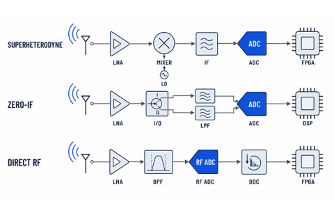
A/D: Moving the digitization point closer to the antenna reduces some analog stages while increasing demands on conversion, clocking, filtering, and digital processing.
Why the Location of Digitization Changes the Entire Receiver
Where you place the ADC determines far more than the required sampling rate. The digitization point changes what the analog front end must accomplish, which impairments you must correct, how much data the FPGA must receive, and where filtering and frequency selection occur. Moving conversion closer to the antenna can increase flexibility, but it also transfers more responsibility to the converter, clock tree, and digital backend.
You can compare the three receiver architectures by following what happens before the signal reaches the ADC.
ADC at IF
RF → Mixer → IF Filter → ADC
The mixer and analog filters complete frequency translation, channel selection, image rejection, and out-of-band blocker suppression before conversion.
Your ADC therefore sees a controlled IF band and can prioritize IF dynamic range instead of direct RF bandwidth.
ADC at I/Q Baseband
RF → I/Q Mixer → I ADC / Q ADC
An analog I/Q mixer translates the selected RF channel close to DC, allowing each converter to process only the required baseband bandwidth.
Lower ADC bandwidth comes with new concerns, including DC offset, I/Q imbalance, LO leakage, and low-frequency noise.
ADC after the RF Front End
LNA → BPF → RF ADC → DDC
The converter directly processes RF or high-IF signals, while channel selection and downconversion move into programmable digital logic.
You now need wide analog input bandwidth, low aperture jitter, strong RF-frequency SFDR, and a high-speed digital interface.
The location of digitization determines whether your converter must prioritize baseband precision, IF dynamic range, or multi-gigahertz input bandwidth. Because different families of Analog-to-Digital Converters (ADCs) are optimized for different combinations of resolution, bandwidth, latency, noise, and power, you should match the converter architecture to the complete receiver signal chain rather than select it from sampling rate alone.
Superheterodyne Receivers: Maximum Analog Control
A superheterodyne receiver is not simply an older architecture waiting to be replaced. It remains a strong choice when you need analog selectivity, predictable frequency planning, and reliable operation in the presence of strong blockers. Its defining advantage is the ability to control the signal environment before the waveform reaches the ADC.
Signal Path
Antenna → LNA → RF Filter → Mixer + LO → IF Filter → IF Amplifier → ADC
The mixer combines the incoming RF signal with a local oscillator and moves the desired channel to a fixed intermediate frequency. At that IF, you can use selective filters and controlled gain stages to complete channel isolation, image rejection, gain control, and blocker attenuation before conversion. The ADC therefore receives a narrower and more predictable spectral window.
Strong Analog Selectivity
RF and IF filters can suppress unwanted energy before it consumes ADC dynamic range.
Lower ADC Input Frequency
Your converter processes the selected IF band instead of the original high-frequency carrier.
Achievable Clock Requirements
A lower ADC input frequency generally reduces the SNR penalty caused by the same clock jitter.
Predictable Signal Planning
Mixing, filtering, and gain are assigned to separate stages with clearly defined performance limits.
What You Trade Away
● More analog components
● Additional LOs
● Image planning
● Mixer spurs
● Larger PCB area
● Reduced flexibility
Where It Still Fits Best
Consider this architecture for narrowband communications, strong-blocker environments, high-selectivity instruments, stable frequency plans, and systems with limited FPGA or high-speed interface resources.
The enduring value of a superheterodyne receiver is not maximum digital flexibility. It is your ability to shape and protect the spectrum before it reaches the ADC.
Zero-IF Receivers: Integration with Baseband Trade-Offs
A zero-IF receiver moves the selected RF channel directly to baseband instead of passing it through a dedicated intermediate-frequency stage. The local oscillator is normally placed at or very close to the target carrier frequency, so the mixer output falls around DC. Separate I and Q paths preserve the amplitude and phase information you need to reconstruct and demodulate the signal.
Zero-IF Signal Path
Antenna → LNA → I/Q Mixer + LO → Baseband Filters → I ADC / Q ADC
Because frequency conversion occurs before sampling, your baseband ADCs only need to cover the occupied channel bandwidth. This can significantly reduce converter speed and digital data rate compared with direct RF sampling. It also makes it practical to integrate the LNA, mixer, PLL, baseband filters, and ADCs into a compact transceiver IC.
No Dedicated IF Stage
You can remove IF filters, IF amplifiers, and some frequency-conversion components.
Lower ADC Bandwidth
The I and Q converters process the channel bandwidth rather than the full RF carrier frequency.
High Integration
The complete receiver can be integrated into fewer ICs with shorter analog connections.
Compact Radio Design
This architecture fits cellular, IoT, and other size- or power-constrained wireless systems.
The Baseband Impairments You Must Control
● DC Offset: Self-mixing and device mismatch can hide weak signals near DC.
● LO Leakage: LO energy can leak into the RF path and return through the receiver.
● I/Q Imbalance: Gain or phase mismatch reduces image rejection and modulation accuracy.
● Low-Frequency Noise: 1/f noise becomes more important when useful signals sit close to DC.
● Calibration Dependence: Digital correction is often required for DC, gain, and phase errors.
Zero-IF is most attractive when you need an integrated wireless transceiver, compact low-power receiver, or cellular and short-range radio supported by mature I/Q calibration algorithms.
A superheterodyne receiver places complexity in the analog IF chain. Zero-IF removes much of that chain, but transfers part of the challenge to I/Q accuracy and baseband calibration.
Direct RF Sampling: Moving Frequency Conversion into the Digital Domain
Direct RF sampling moves digitization closer to the antenna. Instead of using an analog mixer to translate every desired carrier to IF or baseband, you allow a wideband converter to sample the RF carrier or a high-IF band directly. Frequency selection and downconversion then take place inside the ADC or downstream digital logic.
Direct RF-Sampling Signal Path
Antenna → LNA → Bandpass Filter → Balun / Driver → RF ADC → DDC / NCO → FPGA / SoC
After conversion, the full-rate digital stream passes through a numerically controlled oscillator and a digital complex mixer. The selected band is translated to baseband or low IF, while decimation filters limit its bandwidth and reduce the output sample rate. The resulting I/Q data can then be transported to your FPGA or SoC without carrying the entire original sampling bandwidth.
Programmable Frequency Selection
You can change the NCO frequency through software or register settings instead of redesigning an analog LO plan.
Multiple Digital Channels
A converter with multiple DDCs can extract several carriers or sub-bands from the sampled spectrum.
Digital Channelization
The analog front end no longer carries the full responsibility for carrier selection and bandwidth reduction.
Direct RF sampling can reduce the number of analog frequency-conversion stages, but the ADC, clock source, RF filter, and digital backend must be evaluated as one connected system. Engineers who need a deeper implementation reference can review RF-Sampling ADCs for Direct RF-to-Digital Conversion, which brings Nyquist-zone planning, clock-jitter limits, RF input matching, DDC/NCO configuration, and JESD204 data flow into a single design framework.
● Software-Defined Tuning: Reconfigure center frequencies for different channels or standards.
● Multi-Band Processing: Extract multiple occupied bands from one wideband sampled input.
● Fewer Analog Stages: Reduce mixers, IF amplifiers, and part of the analog LO chain.
● Digital Calibration: Measure and compensate channel gain, phase, and delay digitally.
● Channel Synchronization: Support MIMO, beamforming, and phased arrays with synchronized clocks and deterministic links.
Direct Sampling Does Not Eliminate Analog Filtering
Your RF front end must still prevent unwanted energy from consuming ADC full-scale range or folding into the observation band.
● Out-of-band blockers
● Alias bands
● Harmonics
● LNA intermodulation
● ADC input level
● Differential balance
The question is not whether direct RF sampling is technically possible, but whether your complete system can support its clocking, dynamic-range, filtering, data-rate, power, and thermal requirements.
The Engineering Trade-Offs That Decide the Architecture
You should compare superheterodyne, zero-IF, and direct RF-sampling receivers against the same system requirements. The right architecture is the one that meets your RF performance targets without creating unrealistic demands elsewhere in the signal chain.
RF Frequency and Instantaneous Bandwidth
Start by separating three specifications that are often confused. Carrier frequency tells you where the signal is located. Analog input bandwidth tells you whether the converter front end can accept that frequency. Instantaneous bandwidth tells you how much spectrum must be captured and processed at one time.
● Carrier Frequency: The RF location of the desired signal.
● Analog Input Bandwidth: The frequency range the ADC input network can receive effectively.
● Instantaneous Bandwidth: The spectrum your system must observe simultaneously.
A signal centered at 3 GHz does not necessarily occupy 3 GHz of bandwidth, but a direct-sampling ADC must still maintain suitable input performance at 3 GHz. Superheterodyne receivers first translate the desired bandwidth to IF, zero-IF receivers sample only the I/Q baseband, and direct RF receivers process the carrier at its original RF location. Maximum sample rate does not automatically equal usable RF input bandwidth.
SNR, ENOB, and SFDR
● SNR: Shows how converter noise limits your ability to detect and measure weak signals.
● ENOB: Expresses the converter’s effective resolution after noise and distortion are included.
● SFDR: Measures the separation between the desired signal and the largest unwanted spur.
For RF sampling, verify these values at your actual input frequency rather than relying on low-frequency or baseband specifications. Performance can fall as input frequency rises, even when the maximum sampling rate remains unchanged.
Your system SFDR is also affected by LNA-generated IM3, mixer conversion spurs, ADC harmonics, interleaving products, and out-of-band blockers that alias into the selected channel. System-level dynamic range is created by the entire receiver chain, not the ADC alone.
Clock Jitter and Phase Noise
Sampling-time uncertainty converts directly into phase error. As the input frequency rises, the same clock jitter causes a larger reduction in achievable SNR.
SNRjitter = −20 log10(2πfinσt)
Direct RF sampling is therefore more sensitive to the reference oscillator, PLL, clock buffer, PCB distribution, and ADC aperture jitter. IF and baseband sampling generally relax these requirements because the signal reaches the converter at a lower frequency. Your clock budget should always be calculated from the highest intended ADC input frequency, not only from the sampling rate.
Image, Alias, and Filter Planning
Every receiver architecture requires frequency planning, but each one encounters different unwanted spectral products.
Superheterodyne
You must plan around mixer image frequencies, LO harmonics, IF aliases, and mixer-generated spurs.
Zero-IF
Traditional IF images are reduced, but image rejection depends on I/Q balance, LO leakage, and DC-related interference.
Direct RF Sampling
You need a complete Nyquist and alias map covering the desired band, higher Nyquist zones, folded blockers, clock spurs, harmonics, and guard bands.
Front-End Linearity and Blocker Handling
A superheterodyne receiver can progressively attenuate blockers through RF and IF filters. Zero-IF must keep its mixer and baseband stages linear under strong inputs. A direct RF-sampling receiver must protect ADC full-scale range and SFDR, which often means retaining an RF preselector or bandpass filter.
● LNA IP3
● HD2 and HD3
● Compression point
● ADC full-scale range
● Crest factor
● Multi-carrier loading
Digital Output and FPGA Resources
Moving conversion toward RF increases the amount of raw data your digital platform must receive. Use the following relationships for an early interface estimate:
Raw ADC Payload: Data Rate ≈ Fs × Nbits × Nchannels
Complex DDC Output: Data Rate ≈ (Fs ÷ M) × Nbits × 2
Here, M is the decimation ratio and the factor of two represents the I and Q streams. Actual serial lane rates must also account for active DDC channels and interface overhead.
● JESD204B/C lane count
● Maximum SERDES rate
● FPGA transceivers
● DDC output format
● DSP and memory
● Deterministic latency
Removing an analog IF stage may lower analog BOM complexity, but it can increase FPGA, interface, PCB, power, and cooling costs.
Power and Thermal Design
In a superheterodyne receiver, power is distributed across the mixer, LO, IF amplifier, and ADC. Zero-IF usually offers the strongest integration and can be more suitable for low-power radios. Direct RF sampling can require a high-speed ADC, low-jitter clock tree, fast SERDES links, and a larger FPGA workload.
Rising junction temperature can affect SNR, harmonic distortion, channel matching, clock stability, and long-term reliability. Evaluate the receiver at realistic signal levels, duty cycles, ambient temperatures, and airflow conditions.
The architecture decision is complete only when RF performance, digital throughput, power consumption, and thermal behavior can all be supported at the same time.
Side-by-Side Receiver Architecture Comparison
No receiver architecture wins every comparison. Each option places complexity in a different part of your system. Use the table below to identify whether your project is better positioned to manage analog selectivity, I/Q calibration, or high-speed conversion and digital processing.
| Design Factor | Superheterodyne | Zero-IF | Direct RF Sampling |
| ADC input region | IF | I/Q baseband | RF or high IF |
| Analog complexity | High | Medium | Low to medium |
| Digital complexity | Low to medium | Medium | High |
| ADC bandwidth demand | Low to medium | Low | Very high |
| Clock-jitter sensitivity | Lower | Lower | High |
| Analog selectivity | Strong | Moderate | Front-end dependent |
| Image challenge | Mixer image | I/Q imbalance | Nyquist aliases |
| DC offset sensitivity | Low | High | Low |
| Multi-band flexibility | Limited | Moderate | High |
| Raw data rate | Low to medium | Medium | High |
| Calibration requirement | Moderate | High | Moderate to high |
| Strong-blocker tolerance | Strong with filtering | Design-dependent | Requires careful preselection |
| Typical strength | Selectivity | Integration | Bandwidth and flexibility |
Superheterodyne: You accept more analog hardware in exchange for stronger pre-ADC filtering and spectral control.
Zero-IF: You use I/Q calibration to gain integration, compactness, and lower converter bandwidth.
Direct RF Sampling: You invest in clocking, ADC performance, and digital resources to gain wideband flexibility.
Which Architecture Fits Each Application?
Your application determines which trade-offs matter most. Begin with the architecture that best matches your frequency plan, bandwidth, blocker environment, processing resources, and physical constraints, and then verify that choice against real system budgets.
Narrowband Industrial and Telemetry Receivers
● Superheterodyne
● Low-IF
Start here when your frequency bands are stable, channel bandwidth is limited, and FPGA resources are constrained. These systems often value interference rejection and predictable behavior more than wideband software reconfiguration. Analog RF and IF filtering can suppress strong nearby transmitters before they consume converter dynamic range.
Integrated Cellular and Short-Range Radios
Zero-IF is a strong starting point when your target channel bandwidth is clearly defined and you need a compact, highly integrated transceiver. It reduces external IF components and lowers ADC bandwidth. This choice works best when your platform already includes mature correction for DC offset, LO leakage, and I/Q imbalance.
Wideband Software-Defined Radio
● Direct RF Sampling
● High-IF Sampling
Choose these approaches when you need software-controlled frequency selection, multiple simultaneous carriers, or digital channelization. Direct RF sampling gives you the greatest tuning flexibility, while high-IF sampling can reduce clock and converter demands. In both cases, your FPGA must support the required DDC, filtering, interface bandwidth, and memory workload.
5G, MIMO, and Beamforming
● Zero-IF Transceiver
● Direct RF Sampling
Bandwidth alone should not decide this architecture. You must also maintain channel phase alignment, deterministic latency, and stable timing across multiple converters. Evaluate clock distribution, SYSREF strategy, NCO phase reset, multi-ADC synchronization, and total power per antenna channel before selecting the signal chain.
Radar and Spectrum Analyzers
Direct RF Sampling
Direct RF sampling can provide wide instantaneous bandwidth, flexible observation windows, digital spectral analysis, and fewer analog tuning stages. However, you should validate SFDR, phase noise, clock-related spurs, blocker response, and thermal drift. A wide input bandwidth is useful only when weak echoes or signals remain visible beside stronger spectral components.
Cable and DOCSIS Receivers
RF sampling can capture a broad cable spectrum and digitally extract multiple QAM or OFDM channels without duplicating analog receiver chains. Your design still needs wide analog input bandwidth, high ENOB, strong multi-tone linearity, and an output data rate the FPGA can manage. Test with realistic channel loading instead of relying only on a single-tone FFT.
Treat these recommendations as starting points. Your final choice must still survive the actual blocker profile, clock budget, data-rate calculation, thermal environment, and synchronization requirements of your application.
A Step-by-Step Architecture Selection Workflow
A reliable architecture decision begins with system requirements, not a preferred converter or receiver topology. Work through the following sequence before committing your schematic, clock tree, FPGA, or PCB layout.
Define the RF Environment
Record the minimum and maximum RF frequencies, number of operating bands, channel bandwidth, required instantaneous bandwidth, and simultaneous carrier count. This tells you whether a fixed IF plan is sufficient or whether software-defined tuning and multi-band capture are essential.
● RF range
● Bands
● Channel bandwidth
● Carrier count
Define Signal-Quality Requirements
Translate modulation, measurement accuracy, and detection requirements into minimum SNR, ENOB, SFDR, EVM, and noise-figure targets. Add a realistic blocking profile. These requirements determine how much noise, distortion, and unwanted energy the complete receiver can tolerate.
● SNR
● ENOB
● SFDR
● EVM
● Blocking profile
Build a Frequency and Spur Map
Map desired channels alongside image frequencies, Nyquist zones, LO and clock harmonics, intermodulation products, and guard bands. This shows which unwanted products can overlap your observation window and how much RF, IF, or anti-alias filtering you need.
● Images
● Nyquist zones
● Harmonics
● IM products
● Guard bands
Calculate the Clock Budget
Use the highest ADC input frequency and target SNR to calculate the maximum allowable total jitter. Allocate that limit across the reference oscillator, PLL or synthesizer, clock buffer, PCB distribution, and ADC aperture jitter. If the budget is unrealistic, move conversion to a lower IF or baseband.
● Reference
● PLL
● Clock buffer
● PCB distribution
● Aperture jitter
Model the Digital Data Path
Calculate the raw ADC payload, DDC output rate, JESD204 lane requirement, and FPGA SERDES utilization. Include processing, memory, synchronization, and deterministic-latency resources. This step reveals whether reducing analog hardware creates an impractical digital throughput burden.
● Raw data
● DDC output
● JESD lanes
● SERDES
● DSP and memory
Compare Power and Physical Constraints
Combine converter, clock-tree, FPGA, and front-end power instead of comparing ADC power alone. Check package size, PCB layer requirements, copper area, airflow, and cooling. A highly flexible architecture may still be unsuitable if it cannot maintain RF performance at your maximum junction temperature.
● Power
● Package
● PCB layers
● Cooling
● Airflow
Prototype Under Realistic Conditions
Do not approve the architecture from a single moderate-level tone. Test it with the conditions that can expose actual receiver limits.
● Two-tone testing
● Multi-carrier testing
● Blocker injection
● Temperature testing
● Clock-spur testing
● Channel synchronization
Common Architecture-Selection Mistakes
Receiver projects often fail because one attractive specification is allowed to dominate the architecture decision. You can reduce redesign risk by checking the complete signal chain before selecting the ADC, clock system, interface, and front-end topology.
Selecting an ADC Only by Sample Rate
A converter may sample fast enough while still delivering insufficient SNR, ENOB, or SFDR at your target RF input frequency. Check performance curves under the frequency and amplitude conditions your receiver will actually use.
Assuming Direct Sampling Eliminates Analog Filters
Direct RF sampling removes some analog frequency-conversion stages, but it does not remove the need for RF filtering. You must still attenuate blockers, harmonics, and external energy that could alias into the desired observation band.
Comparing Datasheet Numbers from Different Conditions
SNR and SFDR figures are meaningful only when their test conditions are comparable. Before ranking devices, confirm:
● Input frequency
● Sample rate
● Amplitude
● Clock source
● DDC mode
● Temperature
Ignoring Representative Blockers
A clean single-tone FFT does not prove that your receiver will preserve SFDR under real loading. Test with two-tone, multi-carrier, and strong-blocker conditions that represent the intended RF environment.
Underestimating Interface Complexity
A high-speed ADC may require more JESD204 lanes, faster SERDES, careful SYSREF distribution, deterministic-latency configuration, and additional FPGA resources. Calculate the complete data path before finalizing the converter.
Choosing the Newest Architecture
Direct RF sampling offers exceptional flexibility, but it may not be the best answer for every cost, power, thermal, or dynamic-range target. Choose the architecture that fits your requirements, not the one that appears most advanced.
Final Decision: Put Complexity Where You Can Control It
Every receiver architecture contains complexity. Your decision determines where that complexity appears and which engineering disciplines must control it.
Superheterodyne: You manage complexity through analog mixing, frequency planning, and selective RF and IF filtering.
Zero-IF: You reduce the IF chain but take responsibility for I/Q accuracy, DC offset, LO leakage, and digital calibration.
Direct RF Sampling: You move more responsibility into the ADC, low-jitter clock tree, DDC, high-speed interface, and FPGA processing chain.
The best receiver architecture is not necessarily the one with the fewest analog components or the highest sampling rate. It is the architecture that places noise, selectivity, calibration, bandwidth, and processing demands in the domains your engineering team can control most effectively.
Frequently Asked Questions
These answers address the practical questions you are most likely to encounter when comparing superheterodyne, zero-IF, and direct RF-sampling receiver architectures.
Is direct RF sampling always better than superheterodyne?
No. Direct RF sampling gives you greater frequency flexibility, wider digital channelization, and fewer analog conversion stages. However, it also places stricter demands on ADC input performance, clock jitter, RF filtering, JESD204 throughput, FPGA resources, power, and thermal design. A superheterodyne receiver may still provide better selectivity and blocker protection when your frequency plan is stable and the required bandwidth is limited.
What is the difference between zero-IF and direct RF sampling?
A zero-IF receiver uses an analog I/Q mixer to translate the selected RF channel directly to baseband before sampling. Separate I and Q ADCs then digitize the baseband signals. A direct RF-sampling receiver sends the RF or high-IF signal directly into a wideband ADC and performs frequency translation digitally through an NCO, complex mixer, and DDC.
Can an ADC directly sample a carrier above its Nyquist frequency?
Yes, if the signal and converter satisfy the conditions for bandpass sampling or undersampling. A narrow RF band in a higher Nyquist zone can intentionally alias into the first Nyquist zone for digital processing. You must verify the ADC’s analog input bandwidth, the aliased band location, spectral inversion, guard bands, and front-end filtering so that unwanted signals do not overlap the desired band after sampling.
Does a direct RF-sampling receiver still need an anti-alias filter?
Yes. Direct sampling does not prevent out-of-band energy from folding into your observation bandwidth. You still need an anti-alias filter, bandpass filter, or RF preselector to attenuate unwanted carriers, harmonics, noise, and strong blockers. The filter should be designed from the complete Nyquist and alias map rather than from the desired channel bandwidth alone.
Why is clock jitter more important in direct RF sampling?
Sampling jitter creates timing uncertainty, which becomes phase error in the digitized waveform. The same timing error causes greater SNR degradation as the ADC input frequency increases. Because a direct RF-sampling converter processes a much higher input frequency than an IF or baseband ADC, your reference oscillator, PLL, clock buffer, PCB distribution, and ADC aperture jitter must all meet a tighter combined budget.
When should you keep an IF stage?
Keep an IF stage when you need strong analog selectivity, predictable blocker suppression, or a lower ADC input frequency. It is also sensible when your converter or clock system cannot meet direct RF requirements, your FPGA interfaces are limited, or your fixed operating band does not benefit from extensive software reconfiguration. An IF stage can reduce ADC bandwidth, relax jitter limits, and protect dynamic range before conversion.